Service hotline
86+512-62868988

Xinku Liu and his team reported the vertical GaN Schottky barrier diodes (SBDs) on 2” freestanding (FS) GaN wafer from Suzhou Nanowin Science and Technology Co.,Ltd. In the SBDs they developed.
2018-6-13 11:14:35
Recently, Caroline B Lim and her team published a paper in Japanese Journal of Applied Physics, in which the nonpolar m-oriented GaN:Si/Al(Ga)N heterostructures grown on free-standing GaN for intersubband optoelectronics in the short-wavelength, mid- and far-infrared ranges Were assessed
2018-6-13 11:13:34
Recently, a well-known nitride group of University California at Santa Barbara(UCSB)* published an interesting result from measuring the radius of curvature and the threading dislocation density of the commercial 2”
2018-6-13 11:10:18
Gallium Nitride (GaN) is a compound semiconductor material which possesses notable advantages over the conventional semiconductor materials such as Silicon, Silicon Carbide, Aluminum, and so on. This material is most commonly used in optoelectronic products such as Lasers, LEDs.
2018-6-13 11:04:35
GaN-on-silicon will lead with 90% of the market; GaN on silicon carbide will gain traction in transportation but GaN-on-GaN will be hobbled by high prices, Lux Research says
2018-6-13 11:03:18
In 2007, Prof. Zhonglin Wang pointed out the so-called piezotronic effect based on the observation of the local Schottky-barrier height (SBH) modulated by the strain along the piezoelectric direction, i.e. the c-axis of ZnO.
2018-6-13 11:02:11
Overall, 2020 could see an estimated device market size of almost $600M, leading to approximately 580,000 x 6 wafers to be processed. Ramp-up will be quite impressive starting in 2016.
2018-6-13 11:00:44
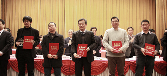
In 2013, the results of suzhou top 10 charming science and technology figures were officially announced by suzhou municipal talent office, municipal propaganda department, municipal science and technology bureau, municipal people's social bureau and municipal science and technology association...
2018-6-10 13:58:23